Research Science Center “Kurchatov Institute”. Federal State Budget Agency “State Research Center of Russian Federation – Institute of Theoretical and Experimental Physics.”FSBA SRC RF – ITEP”, 117218, Russia, Moscow, B. Cheremushkinskaya Street 25,
e-mails: grafutin@itep.ru,
epprokopiev@mail.ru, elnikova@itep.ru , spt@mail.ru
The report proves that one of the effective methods to define sizes of nanodefects (vacancies, clusters of vacancies), free pore volumes, cavities and holes, and their concentration and chemical composition in annihilation space in nanomaterials and other technically important materials, is positron annihilation spectroscopy. Here, we briefly reviewed the experiments for nanodefects in porous silicon, silicon and monocrystals and in quartz powders, irradiated by protons, as well as in metals and alloys, irradiated by protons and neutrons.
INTRODUCTION
Positron annihilation spectroscopy (PAS) (Goldanskii, 1968; Grafutin, Prokopiev, 2002; Prokopiev, Timoshenkov, Grafutin et al.,1999), allowing to define both electronic structure of perfect crystals and various imperfections of especially small sizes in solids and porous systems, such as vacancies, clusters of vacancies and free volumes up to one cubic nanometer, comprises three basic methods: studying of time distribution of annihilation photons (TDAP), angular distribution of annihilation photons (ADAP) and Doppler width of annihilation lines with energy 0.511 МeV (DWAL) (Goldanskii, 1968; Grafutin, Prokopiev, 2002). TDAP method gives data on electronic density in positron annihilation place and ADAP and DWAL methods give information on distribution of electron impulses and on chemical compound of the environment surrounding nanoobjects in annihilation place. There are two groups of PAS methods. In the first group there are used slow positrons that allow to investigate surface layers on small depths. In the second group there are used fast positrons that can get into an investigated object on greater depths  µm and give information on the type, concentration and distribution of defects in the whole volume of a solid. All these methods have already received wide application for research in modern material science, particularly in nuclear and electronic material science (see, for e.g., Wurschum, Schaefer 1996; Druzhkov, Perminov, 2007; Gusev, 2005; Wurschum, Schaefer, 1996; Arefiev, Vorobiev, Prokopiev, 1983; Krause-Rehberg, Leipner 1999; Arefiev, Prilipko, Prokopiev et al, 1983; Batavin, Druzhkov, Garnak et al. 1980; Prokopiev, 1993; Fedorov, Prilipko, Prokopiev et al., 1982; Prilipko, Prokopiev, 1980; Britkov, Gavrilov, Grafutin et al.,2004; Grafutin V.I., Ilyukhina O.V., Kalugin et al., 2006; Gavrilov, Grafutin, Ilyukhina et al., 2005; Prokopiev, 1996; Jean, 1990 ; Gregory Roger, 1991; Varisov, Grafutin, Zaluzhnyi et al., 2007; Eldrup, Lightbody, Sherwood, 1991; Shantarovich, Yampolskii, Kevdina, 1994; Prokopiev, Grafutin, Timoshenkov et al., 2008 ; Britkov, Gavrilov, Grafutin et al., 2007; Grafutin, Ilyukhina, Myasishcheva, 2005; Grafutin, Zaluzhnyi, Timoshenkov et al., 2008; Kozlov, Kozlovskii, 2001; Kozlov, Kozlovskii, Lomasov, 2000; Grafutin, Zaluzhnyi, Timoshenkov et al., 2008; Prokopiev, 1990).
The researches of positron annihilation in compacted nanocrystal metals and alloys (Grafutin, Prokopiev, 2002; Prokopiev, Timoshenkov, Grafutin et al.,1999; Schaefer, 1993; Gusev, 2005; Arefiev, Prilipko, Prokopiev et al, 1983; Wurschum, Schaefer 1996; Arefiev, Vorobiev, Prokopiev, 1983), and also in semiconductors (Krause-Rehberg, Leipner 1999; Batavin, Druzhkov, Garnak et al. 1980; Prokopiev, 1993; Fedorov, Prilipko, Prokopiev et al., 1982; Prilipko, Prokopiev, 1980; Britkov, Gavrilov, Grafutin et al.,2004; Grafutin, Ilyukhina, Kalugin et al. 2006) and porous silicon (Gavrilov, Grafutin, Ilyukhina et al., 2005) have yielded the following basic results (Goldanskii, 1968; Prokopiev, Timoshenkov, Grafutin et al.,1999; Schaefer, 1993; Gusev, 2005; Wurschum, Schaefer, 1996):
1.Lifetimes of positrons in compacted nanocrystal metals and alloys as well as in elementary Ge and Si semiconductors subjected to irradiation by various elementary particles and γ beams differ from lifetimes of free positrons τf in ideal crystals (Gusev, 2005).
2. The share of positrons grasped by vacancies, grows with increase in pressure in case of metals and alloys as well as with increase in doze of irradiation in case of semiconductors. In the first case it means that the increase in pressure leads to the growth of area of section (interfaces) borders, and in case of semiconductors – to the increase in concentration of dot defects with nanometer sizes (Gusev, 2005).
3. In nanomaterials based on metals and alloys positrons are mainly grasped by monovacancies and divacancies on the section border of two adjacent grains (in joints of grains), and also by nanopores, that are the joints of three adjacent crystal particles and free volumes of absent crystal particles. These conclusions are made on the basis of measurements of positron lifetimes in compacted metals and alloys (Gusev, 2005; Prokopiev, 1990). In these samples lifetime τ1 is close to lifetime τN in crystal lattice vacancies in a volume of metal. It is generally accepted that the shortest lifetime τ1 experimentally fixed in TDAP spectra, is caused by positron annihilation in vacancies on the border of grain section (the interface vacancies) with sizes < 0.2–0.4 nm. Intermediate lifetime τ2 characterizes positron annihilation in three-dimensional vacancy agglomerates (nanopores whose size reaches 10 removed atoms ≈0.6–0.8 nm). Very long lifetime τ3 corresponds to positron annihilation in pores – free volumes whose size is close to the size of crystal particles  nm. It enables to study the structure of section borders, which defines alongside with the small sizes of grains the majority of properties of nanomaterials.
4. In irradiated semiconductors and pore systems (Goldanskii, 1968; Grafutin, Prokopiev, 2002; Prokopiev, Timoshenkov, Grafutin et al.,1999; Prokopiev, 1993; Arefiev, Prilipko, Prokopiev et al, 1983; Fedorov, Prilipko, Prokopiev et al., 1982Prilipko, Prokopiev, 1980; Britkov, Gavrilov, Grafutin et al.,2004; Grafutin, Ilyukhina, Kalugin et al. 2006; Britkov, Gavrilov, Grafutin et al, 2007; Grafutin, Ilyukhina, Myasishcheva, 2005; Grafutin, Zaluzhnyi, Timoshenkov et al., 2008; Grafutin, Zaluzhnyi, Timoshenkov et al., 2008) positrons are grasped by dot defects with average size  nm and by pores with average size
  of nm mainly of monovacancy and divacancy type and to a lower degree of tetra-, penta-and hexavacancy type as the most widespread among other radiating defects, for example, in silicon.
5. Free vacancy volumes grasping positrons at low temperatures in metals and alloys belong to section borders rather than to crystal particles (Gusev, 2005).
6. The capture of positrons by crystal particles in metals and alloys is unlikely as plastic deformation of metals leads to smaller change of lifetime of positrons than in compacted nanocrystal metals (Gusev, 2005).
For the time being it is experimentally proved that positrons effectively probe free volumes (basically vacancies and divacancies) with sizes  nm both in metals and alloys, and in semiconductors and pore systems and nanocrystal compacted materials (Goldanskii, 1968; Prokopiev, Timoshenkov, Grafutin et al.,1999; Gusev, 2005; Prokopiev, 1993; Fedorov, Prilipko, Prokopiev et al., 1982; Prilipko, Prokopiev, 1980; Arefiev, Prilipko, Prokopiev et al, 1983; Britkov, Gavrilov, Grafutin et al.,2004; Grafutin, Ilyukhina, Kalugin et al., 2006; Britkov, Gavrilov, Grafutin et al, 2007; Grafutin, Ilyukhina, Myasishcheva, 2005; Grafutin, Zaluzhnyi, Timoshenkov et al., 2008; Grafutin, Zaluzhnyi, Timoshenkov et al., 2008; Prokopiev, 1990).However, other direct methods including transmission electronic microscopy of high resolution and diffusion of atoms hardly give the opportunity to study interfaces. PAS methods sensitivity concerning the contents of positron sensitive defects thus is limited to ≥1014–1015cm-3.
The study says (Gusev, 2005) that up to now there has not been investigated (or understood) the question on the structure of interfaces and their nuclear density, on the influence of nanopores and other free volumes on the properties of nanomaterials. Therefore one of the main purposes of works on research of nanomaterials by positron method is in the establishment of correlations between the nature, the sizes and concentration of nanoobjects and the quality of modern materials used in practice. For this purpose there can bee used various methods so that to search for such correlations.
Below there are being examined methods defining the sizes of nanoobjects, their concentration and a chemical composition of the environment surrounding nanoobjects, on experimentally measured parameters of TDAP and ADAP spectra for positrons annihilated in porous systems and in elementary semiconductors of Ge and Si type subjected to irradiation by various elementary particles and  beams and other technically important materials on the basis of the theoretical grounds developed in (Prokopiev, 1996; Jean, 1990; Gregory Roger, 1991; Varisov, Grafutin, Zaluzhnyi et al., 2007; Eldrup, Lightbody, Sherwood, 1991; Shantarovich, Yampolskii, Kevdina, 1994; Prokopiev, Grafutin, Timoshenkov et al., 2008) and various examples of their applications.
DEFINITION OF SIZES OF VACANCY FREE VOLUMES, PORES, HOLES IN POROUS SYSTEMS AND NANOMATERIALS AND OTHER TECHNICALLY IMPORTANT MATERIALS
Usually for calculations of the pore size there is used a simple model in which the cavity is modeled by a spherical hole with an infinite potential barrier of radius R0. Positron and positronium are in this cavity and annihilate in it. Thus parapositronium (p-Ps) annihilates mainly on its own electron, and orthopositronium (o-Ps) and positron annihilate on electrons of the environment surrounding the cavity. To provide the possibility of pick-of annihilation it is postulated that in border area with size ΔR there happens the overlapping of wave functions of positron and the positron which is the part of o-Ps with wave functions of environment electrons. Thus the radius of pore free volume R will equal ΔR=R0–R.
Simple quantum-mechanical calculations allow to correlate the lifetime of positron and orthopositronium o-Ps in the cavity  with the size of the cavity
R0 and ΔR (Jean,1990)
 (1)
(1)
In this formula  ns (Dannefaer, 1987) is meaningful for the lifetime positron or
  ns is an average of spins
positronium lifetime
in the environment volume (outside of a pore or a vacancy) (Jean, 1990; Gregory Roger, 1991; Varisov, Grafutin, Zaluzhnyi et al., 2007; Eldrup, Lightbody, Sherwood, 1991; Shantarovich, Yampolskii, Kevdina, 1994; Prokopiev, Grafutin, Timoshenkov et al., 2008).
The analysis of o-Ps annihilation in materials with definite values of radii of pores in molecular solids and zeolites on the basis of the equation (1) has shown (Jean,1990), that value ΔR=R0–R=1.66Å. Generally speaking, ΔR depends on the substance nature. Therefore in this case equation (1) for silicon and quartz probably can be applied only to estimate the sizes of pore radiuses. It should be mentioned that TDAP spectroscopy has turned out an extremely effective method of defining the sizes of pores and micropores and pore distribution along the radiuses in porous systems (adsorbents, zeolites, molecular solid substances, etc.) (Gusev, 2005; Prokopiev, 1996; Jean, 1990; Gregory Roger, 1991; Varisov, Grafutin, Zaluzhnyi et al., 2007; Eldrup, Lightbody, Sherwood, 1991; Shantarovich, Yampolskii, Kevdina, 1994; Prokopiev, Grafutin, Timoshenkov et al., 2008).
We shall apply the same quantum model of Ps with the purpose to establish dependence between the experimental values  (FWHM(full width half-maximum)) of narrow components of ADAP and radius of free volume R. In this case the parity between
  and
and  for p-Ps is as follows (Jean, 1990)
  , (2)
, (2)
where R, ΔR and  are expressed in Å and mrad correspondingly. Using equations (1), (2), we can estimate radiuses of free volumes in porous systems, defective materials and nanomaterials on measurement of sizes
  of narrow components by ADAP method. We shall note that in cases with silicon and quartz for the parity between R and
  it is rational to use the approximate formula
 , (3)
, (3)
as value  for silicon and quartz in case of p-Ps have not been found in other studies. In formula (3),
  denotes a width of narrow components in ADAP spectra defined by movement of the center of p-Ps weights.
The advantage of ADAP method in comparison with TDAP method is that ADAP method gives orientation dependence of R (along the direction of measured impulses) while TDAP method gives average values of R. But the measurements of ADAP spectra takes more time than TDAP method. Below there are given data on the definition of the sizes of nanoobjects and their concentration by ADAP method for porous silicon, silicon and monocrystals of quartz irradiated by protons, as well as in powders of quartz on the basis of stated above calculation methods and the experimental data received earlier (Grafutin, Prokopiev, 2002; Prokopiev, Timoshenkov, Grafutin et al., 1999; Britkov, Gavrilov, Grafutin et al., 2004; Grafutin, Ilyukhina, Kalugin et al., 2006; Gavrilov, Grafutin, Ilyukhina et al., 2005; Britkov, Gavrilov, Grafutin et al., 2007; Grafutin, Ilyukhina, Myasishcheva et al., 2005; Grafutin, Zaluzhnyi, Timoshenkov et al., 2008; Grafutin, Zaluzhnyi, Timoshenkov et al., 2008), and in a number of new experiments in monocrystals and powders of quartz.
DEFINITION OF RADII OF PORES AND THEIR CONCENTRATION IN POROUS SILICON
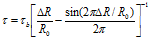
Data of fig.1, 2 and tab. 1 fig.1 show presence p-Ps in porous silicon (see, for example, the sample of porous silicon PR86 (tab.1) and fig.2).
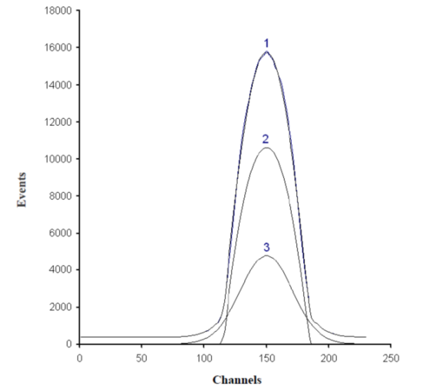
Fig.1. Angular distributions of annihilation photons in monocrystal samples of silicon: Si-monocrystal, mirror, p-type, orientation <111>, SDB – 10, h = 340 µm): 1 – ADAP curve plotted on experimental points 2,3 – parabolic and gauss components of the spectrum respectively. The X-axis shows channels of the analyzer (the value of the channel 0.2 mrad), the Y-axis shows the number of even


Fig. 2. Angular distributions of annihilation photons in pore samples of silicon: Si – pore; <111>; SDB – 0.03; h = 360 – 370 µm;
HF:C2H5OH = 2 : 1; porosity 45 % ± 3 %; (2 of gauss + parabola) (see tab.1)): 1 – total spectrum (the sum of spectra 3, 4, 5), 2 –ADAP curve plotted on experimental points, 3 – the first gauss component of spectrum, 4 – parabolic component of spectrum, 5 – the second gauss component of spectrum, points – experiment. The X-axis shows channels of the analyzer (the value of the channel 0.2 mrad), the Y-axis shows the number of events.
Table 1
Parameters of investigated samples of porous silicon, features of their production and characteristic of ADAP spectra
|
Sample |
Sample characteristics |
Ig2=Sg1/Ssum |
Ig1=Sg1/Ssum |
Ip=Sp/Ssum |
Note |
|
PR86 |
Pore Si, <111>, SDB-0.03, h=360-370 µm, HF:C2H5OH=2:1, J=20 mA/cm2 |
0.015± 0.003 |
0.493± 0.052 |
0.492± 0.044 |
Porosity 45%±3 % |
Notes: h is thickness of silicon plates, <111> is crystallographic orientation, SDB – 0,03 is the mark of silicon plates alloyed by B with specific resistance 0.03 оm·cм, Ig =
Sgi/Ssum (i=1,2) – intensity of gauss components, and
IP = Sp/Ssum is the intensity of parabolic component in Adap spectra (Ssum is the total area of the Adap spectrum, and Sgi
and
Sp are areas of the gauss and parabolic components in this spectrum respectively). J is the current density.
The experimental ADAP spectra of this sample of porous silicon are well approximated by parabola
(Ip) and by two gausses (Ig1, Ig2). In a defectless crystals of silicon (fig.1) and in a number of porous samples (Britkov, Gavrilov, Grafutin et al., 2007), these spectra are represented by the superposition of parabola and gauss. Positron annihilation characterized by parabolic component can be explained by positron annihilation on electrons of valence zone of silicon. In its turn wide gauss component  is caused by positron and o-Ps annihilation through different channels in a faultless part of a crystal, volume and on the surface of pores, and narrow gauss component
Ig2 is caused by p-Ps annihilation in the volume of pores. The full width of this component on FWHM
half-height makes up (θ1/2)g2=0.8 mrad, which corresponds to kinetic energy of an annihilating electron-positron pair of 0.044 eV, and its intensity of 1.5 %; and general output of Ps in porous silicon reaches 6 %.To define of radiuses Rg2 of pores of width ( θ1/2)g2, there the formula (2) was used. For the experimental value ( θ1/2)g2=0.8 mrad (see above) , there was received an average value of pore radius Rg2≈19.09Å≈2 nm.
The consideration of the kinetic scheme of annihilation disintegrations and transformation p-Ps in a pore layer enables to receive dependence between constant of capture ktr and component intensity Ig2 (Britkov, Gavrilov, Grafutin et al, 2007)
 s-1 . (4)
Here we use  s-1 is a velocity of p-Ps annihilation in the volume of crystal. Thus, the constant of capture speed p-Ps, estimated on the basis of data in tab.1 and formula (4) makes up
  s-1.
s-1.
On the other hand the value of capture speed  can be in its turn defined on the basis of certain expression (Britkov, Gavrilov, Grafutin et al., 2007)
 , s-1 (5)
Here  is a dimensionless value of p-Ps and positron annihilation probability, grasped by defect (Prokopiev, 1990).
 is an average value of capture section by defects of p-Ps or positron;
  is velocity of thermalized p-Ps or positron;
  is an average concentration of defects (in defective area of crystal) sensitive to thermalized states of positron or p-Ps. Thus, from the given expressions, it is possible to define the values of Ng2, if we have such parameters as
  and
and  . The average thermal p-Ps or positron velocity at room temperature
  is estimated with formula
  , cm/s, where
  is the Boltzmann constant,
  is effective p-Ps weight,
  is mass of free positron. From this formula for positron where
  we receive
  cm/s, and for p-Ps where
  –
–  cm/s. From this, it appears that at
  by formula (5)
  cm-3. According to these data it can be supposed that the effective free centers (areas of p-Ps capture) are most likely to be ultramicropores and micropores of closed and open type with sizes ≤2 nm.
DEFINITION OF RADII OF PORES AND THEIR CONCENTRATION IN WAFERS OF SILICON IRRADIATED BY PROTONS
Investigated samples with sizes 10´20´10 mm3 have been cut out from the whole plates of silicon. For researches there have been chosen four samples designated by us as Si 10 (the initial unirradiated sample), Si 14, Si 15 (the samples of silicon irradiated by protons with energy Е and fluence Ф). The parameters of the investigated n- and p – silicon plates, features of their production and the main characteristics of ADAP spectra are given in tab.2-5.
Table 2
Parameters of investigated samples of silicon, special features of their production and characteristic of ADAP spectra
|
Sample |
Sample characteristics |
|
Ig = |
|
IP = Sp/Ssum |
Note |
|
Si 10 |
Si, <100>, SDP – 4.5, h = 455 µm, n – type |
11.0 ± 0.3 |
0.256 ± 0.04 |
6.98 |
0.744 ± 0.049 |
|
|
Si |
Si, <100>, SDP – 4,5 h= 415 µm |
11.1 ± 0.32 |
0.256 ± 0.04 |
6.93 |
0.735 ± 0.051 |
irradiated by protons Е = 40 keV, Ф = 5·1016 cm-2 |
|
Si 14 |
Si, <100>, SDP 2 – 3, h = 418 µm |
11.1 ± 0.27 |
0.283 ± 0.04 |
6.94 |
0.717 ± 0.045 |
irradiated by protons Е = 150 KeV, Ф = 4·1016 cm-2 |
|
Si 15 |
Si, <100>, SDP 2 – 3 h = 418 µm |
11.1 ± 0.28 |
0.293 ± 0.041 |
6.81 |
0.707 ± 0.047 |
irradiated by protons Е = 150 keV, Ф = 4·1016 cm-2 |

 , mrad
 , mrad
Notes: h is thickness of silicon plates, <100> – their crystallographic orientation, SDP – 4,5 is a mark of silicon plates doped by P with specific resistance 4,5 and 2-3 оm·cm, Е and Ф are the energy and the fluence of protons respectively,  , mrad is a width of a gauss component with intensity Ig = Sg/Ssum, and (
 , mrad) is a cutoff angle for the parabolic component with intensity IP = Sp/Ssum
in ADAP spectra (Ssum is a total number of coincidence events, and Sg and
Sp are the coincidence event rates corresponding to the gauss and parabolic components in ADAP curves).
Table 3
Parameters of investigated samples of Si of p-type and features of their production
|
Sample |
Sample characteristics |
Note |
|
164 (1) |
Si-monocrystal, mirror, <111>, SDB-10, h=340 µm. |
11 degree of processing |
|
165 (2) |
Si-monocrystal, mirror, <111>, SDB-10, h=340 µm, is irradiated by protons: Е=3 MeV, Ф=1.03∙1016 cm-2 |
11 degree of processing |
|
163 (3) |
Si-monocrystal, mirror, <111>, SDB-10, h=340 µm, is irradiated by protons: Е=3 MeV, Ф=4.3∙1016 cm-2 |
11 degree of processing |
|
153 (4) |
Si-monocrystal, polished, p-type, <111>, SDB -10/20, h =490 µm, r=9.8-10.0 om×cm |
|
|
166 (5) |
Si-monocrystal, polished, p-type, <111>, SDB-10/20, h=490 µm, r=9.8-10.0 om×cm, is irradiated by protons: Е=3MeV, Ф=5.15∙1015 cm-2 |
|
|
152 (6) |
Si-monocrystal, polished, p-type, <111>, SDB-10, h=500 µm, r=8.6 om×cm |
|
|
154 (7) |
Si-monocrystal, polished, p-type, <111>, SDB-10, h=500 µm, r=8.6 om×cm, irradiated by protons: Е=3 MeV, Ф=6.88∙1015cm-2 |
Bunch is displaced from the center of target by 22 mm. |
|
155 (8) |
Si-monocrystal, polished, p-type, <111>, SDB-10, h=500 µm, r=8.6 om×cm, is irradiated by protons: Е=3 MeV, Ф=7∙1015cm-2 |
Bunch is in the center of target. |
|
162 (9) |
Si-monocrystal, polished, p-type, <111>, SDB-10, h=500 µm, r=8.6 om×cm, irradiated by protons: Е=3MeV, Ф=1.9∙1016cm-2 |
Table 4
Characteristics of ADAP spectra of investigated samples of Si of p-type and parameters OF RADIATION DEFECTS
|
Sample |
Ig=Sg/Ssum |
|
ktr∙10-9, s-1 |
Rg, Å |
Ng∙10-17, cm-3 |
|
164 (1) |
0.335±0.031 |
0.665±0.035 |
|||
|
165 (2) |
0.600±0.030 |
0.400±0.022 |
1.2 |
1.6 |
1.5 |
|
163 (3) |
0.589±0.028 |
0.411±0.021 |
1.15 |
1.6 |
1.4 |
|
153 (4) |
0.330±0.029 |
0.670±0.034 |
1.6 |
||
|
166 (5) |
0.373±0.032 |
0.627±0.034 |
0.19 |
1.6 |
0.2 |
|
152 (6) |
0.305±0.029 |
0.695±0.035 |
|||
|
154 (7) |
0.446±0.049 |
0.554±0.047 |
0.63 |
1.6 |
0.6 |
|
155 (8) |
0.332±0.029 |
0.668±0.035 |
- |
- |
- |
|
162 (9) |
0.512±0.026 |
0.488±0.022 |
0.93 |
1.6 |
1.0 |
Table 5
Parameters of investigated samples OF Si of p-type, feature of their PRODUCTION and characteristics of ADAP spectra
|
Sample |
Sample characteristics |
Ig=Sg/Ssum |
|
Ng∙10-16 cm-3 |
|
164 (1) |
Si-monocrystal, mirror, p-type, <111>, SDB-10, h=340 µm |
0.335±0.031 |
0.665±0.035 |
|
|
153 (4) |
Si-monocrystal, polished, p-type, <111>, SDB-10/20, h =490 µm, r=9.8-10,0 om×sm |
0.330±0.029 |
0.670±0.034 |
1.63 |
|
152 (6) |
Si-monocrystal, polished , p-type, <111>, SDB-10, h =500 µm, r=8.6 om×sm |
0.305±0.029 |
0.695±0.035 |
1.60 |
Notes: h is a thickness of silicon plates, <111> is their crystallographic orientation, SDB-10 and SDB-10/20 are marks of silicon plates doped by B, Е and Ф are the energy and the fluence of protons respectively, Ig = Sg/Ssum is an intensity of gauss component, and
IP = Sp/Ssum is intensity of a parabolic component in ADAP spectra (Ssum is a total area of experimental ADAP spectrum, and Sg and
Sp relate to the area of the gauss and parabolic component respectively).
According to (Britkov, Gavrilov, Grafutin et al., 2004; Grafutin, Ilyukhina, Kalugin et al., 2006, Grafutin, Ilyukhina, Myasishcheva et al., 2005), the difference between the intensities of gauss component Ig
(irradiated), that is the irradiated plates of silicon, and
Ig (unirradiated) (initially unirradiated plate) in ADAP spectra, can be written down in the form of
ΔIg = Ig (irradiated) )–Ig (unirradiated) =  . (6)
. (6)
It means that the average value of capture speed of capture makes

 ΔIg/
ΔIg/ , (7)
, (7)
where
 . (8)
. (8)
In formula (6), τ1 is a short lifetime of positron in a silicon crystal, gi is statistical weight of the i-positron «defective state», contributing to the process of general annihilation. In its turn ktr can be evaluated by formula (3). An average thermal speed of positrons at temperature T was estimated by the formula  , cm/s.
Let’s estimate the value of  , evaluated by expression (4), for
  (see the bottom line in tab.2) (Grafutin, Ilyukhina, Myasishcheva et al., 2005). With this value of
  by formula (3) for the value of τ1=2.19∙10-10 with (Dannefaer, 1987) we will receive
  s-1.
s-1.
The size of vacancies, complexes of vacancies or pores and energy  in the assumption of their spherical geometry in the annihilation place on external valence electrons can be also found by using only ADAP data, In fact, the dispersion σ of gauss component of ADAP spectra approximated by the normal law of error distribution is unequivocally dependant on energy
  of annihilating electron-positron pairs which are in a pore of radius Rg
 , (9)
, (9)
where  mrad. Here
  is a total width of ADAP curve on the half-height. As the majority of works use not the dispersion but the width on the half-height, we will give the expression connecting energy of annihilating electron-positron pair with the full width on the half-height
 (10)
(10)
Here
the energy E is in
eV, and  is a total width of ADAP curve on the half-height, in mrad.
Thus for samples of silicon (see tab.2) the measured value of  makes up 11.1 mrad and it corresponds to energy of annihilating electron-positron pair E=8.5 eV, and, for example, for 11.5 mrad E=9.13 eV. Taking into consideration that before annihilation the positron has time to be thermalized the measured energy is defined mainly by electron energy. The table value of energy for
  of electronic external shell of silicon is
  eV (Babichev, Babushkina, Bratkovsky, 1991). As we can see the correlation of these values of energies
  and
and  is quite satisfactory. Thus, positrons annihilate mainly on external valence electrons of silicon atom of pore “wall”. It is possible to assume that the difference of values
  эВ is caused by the contribution of positron energy in the volume of a potential hole (spherical defect) to the energy of annihilating electron-positron pairs.
Then using equation (1) we have defined for comparison radiuses of free volumes of vacancies according to the measurement lifetime of positrons in the silicon irradiated by electrons and protons by TDAP method (Dannefaer, 1987; Puff, Dannefaer, et al., 1987; Prokopiev, 1987; Prokopiev, 1980; Batavin, Prokopiev, Salmanov et al., 1982). We assumed that for our case enough moderated energies and dozes of protons during the irradiation of plates of silicon are generated mainly to dot defects (Dannefaer, 1987). Lifetimes in mono vacancies remain within the limits from 266 up to 270 ps, in divacancies – within the limits from 300 up to 325 ps, in tetra vacancies; it equals 435 ps, in pent vacancies, it equals 505 ps, and in hex vacancies it makes up about 520 ps (Dannefaer, 1987; (Puff, Dannefaer, et al., 1987; Prokopiev, 1987; Prokopiev, 1980; Batavin, Prokopiev, Salmanov et al., 1982). In fig.3 there is given the diagram of dependence of these values  from
from  plotted by formula (1). The average value of effective radius of radiation defects calculated by formula (1) to the average value lifetime makes up the value of
  Å.
Å.
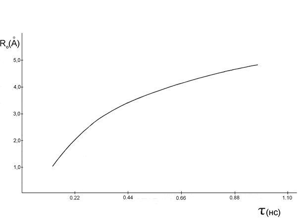
Fig.3. The dependence of positron lifetime in pores from effective radius R0 of pores. The calculation is carried out by the formula (1) for ∆R=1.66 Å (Yean, 1990) and τb=0.219 ns (Dannefaer, 1987).
Thus, if we assume, that in the vacancy (pore) (potential hole) there is a positron instead of positronium, and it annihilates on electrons of wall material, its energy in the hole should be about 0.35 eV at Е = 11.1 eV. As the energy of the particle being in a potential hole is defined by the size of a hole then according to formula (2) the energy of a positron should correspond to a hole with radius Rg ≤10.4 Å for  = and 11.1 mrad. Quite great divergences Rg values defined by TDAP and ADAP methods can be explained either by methodical errors or by the fact that TDAP method defines average values of
  in spherical approach for vacancies while ADAP method can give orientation dependence of Rg (along the direction of measured impulses). According to the microscopy theory of vacancies (for example, for vacancy (Boorguen, Lanno, 1985) in silicon), orientation dependences of electronic properties of vacancy along various crystallographic directions possess significant features. It appears that vacancy has four charge states
  , and only two of them (the latter) can be observed by EPR. Apparently, ADAP method enables to observe orientation dependences of electronic properties of vacancy walls and their sizes depending on crystallographic directions. It is of course necessary to continue thorough researches in this direction. The constant of silicon lattice equals a=5.43 Å, and the average value of interatomic distance in silicon equals rsi=2.087 Å. Thus, the comparison of the values radiuses measured by TDAP method Rg ≈1.7 Å and rsi=2.087 Å says about the satisfactory character of the models used. Then using Rg ≈1.7 Å we define the average value of positron capture section by defects
  cm2. To estimate the average values of concentration of radiation defects by formula (4) we accept
  s-1,
s-1,  cm2 and v≈107 cm/s. Thus we receive the value of concentration of radiation defects in silicon of
  – type with the orientation (100) (Grafutin, Ilyukhina, Myasishcheva, 2005; Grafutin, Ilyukhina, Kalugin et al., 2006) that equals
  cm-3, and in silicon of p-type with the orientation (111) (Britkov, Gavrilov, Grafutin et al.,2004; Grafutin, Ilyukhina, Kalugin et al., 2006),
  cm-3 (see tab.2-5). On the basis of the above-stated it is possible to suppose that in investigated
  -type and p-type silicon plates irradiated by protons there can first of all be found radiation defects of type of monovacancies V and their complexes. It is Dot radiating defects with sizes (diameters) of about from 2 up to 10 Å that are the effective centers of positron capture (Varisov, Grafutin, Zaluzhnyi et al., 2007). Thus, positron method allows to estimate effectively the concentration of dot radiation defects in silicon with sizes
  nm, which is practically inaccessible by means of the existing methods. It should be noted that It was positron methods that allowed to establish the fact that in different defective solids dot defects plays the main role.
Definition of radii of free volumes and their concentration in the monocrystals of quartz irradiated by protons
As it has been shown in our experiments (Grafutin, Zaluzhnyi, Timoshenkov at al., 2008), at the annihilation of completely thermalized p-Ps atoms in monocrystals of quartz in the interval of temperatures 288-633 K the full width of narrow component on its half-height (θ1/2)g2 at the intensity θg2 makes up about (θ1/2)g2 ≈ 1.03–1.25 mrad, and for wide component with intensity Ig1
the full width is θ1/2 ≈ 10 mrad (see tab. 6).
Table 6
Annihilation Parameters of positrons in quartz at different
temperatures
|
Т, K |
|
|
|
|
|
|
633 |
1.25÷0.05 |
0.0300÷ 0.0026 |
10.70÷0.05 |
0.9700÷ 0.0210 |
13.3 |
|
473 |
1.18÷0.04 |
0.0326÷ 0.0021 |
11.00÷0.04 |
0.9674÷ 0.0170 |
14.1 |
|
288 |
1.02÷0.05 |
0.0359÷ 0.0041 |
10.70÷0.09 |
0.9641÷ 0.0320 |
16.3 |
 , mrad
 , mrad


These data allow to speak about the presence of p-Ps in monocrystals of quartz. The general positronium output in quartz reaches 12 %, and its energy is about 0.025 – 0.06 eV. It is necessary to note that interaction delocalized of p-Ps with the crystal lattice of quartz leads to the occurrence of lateral peaks at angles inversely proportional to the value of the vector of reciprocal lattice. At the same time these lateral peaks can’t be observed in monocrystalls of quartz with the highest concentration of impurities (Grafutin, Zaluzhnyi, Timoshenkov at al., 2008).
Evidently, this circumstance says that atom p-Ps in this case is localized in monocrystals of quartz with the highest concentration of impurities or radiation defects in the area of certain volume (cavity) with radius that equals the constant of quartz lattice. The average value of cavity radius (see tab.1) modeled by potential hole with radius R with infinitely high potential barrier in which there occurs  annihilation in quartz estimated by formula (3) given in tab.6. It should be noted that dependence of intensity Ig2=S2/Ssum of the narrow component (tab.6) is enough weak, that in general satisfies the theoretical dependence Ig2 received in works (Goldanskii, 1968; Grafutin, Prokopiev (2002); Prokopiev, Timoshenkov, Grafutin et al.,1999; Grafutin, Zaluzhnyi, Timoshenkov et al., 2008). Here S2 is a coincidence counting rate, that is the area corresponding intensity Ig2 in ADAP spectra, and Ssum is a total number of coincidences. From tab.6 we can see that radiuses of localization of p-Ps atom depend on temperature and vary in temperature interval from 288 K to 633 K from 16,3 Å at 288 K up to 13,3 Å at 633 K. The explanation of such abnormal dependence of R, which is difficult to explain within the framework of the used evaluation model, can be made within the framework of the concept of quasi-particle state of Ps caused by Ps – phonon interaction of this localized atom with oscillatory states of defects of crystal structure (Prokopiev, 1987; Ikari, Fujiwara, 1979). Here the effective weight of Ps decreases with rise of temperature. It is can be nothing but the quantum effect caused by the attenuation of quasi-particle state of positronium in a crystal. Such effect leads to higher values of
  , and consequently to lower R (see equation (2) and tab.5). Then using the data tab.5 we define the concentration of
  capture centers in quartz, where R ≈ 12∙10-8cm, Ig2≈0.03,
  cm-3. According to these data it is possible to suppose that the effective free centers (areas of positronium capture) are most likely to be vacancies or divacancies, which appear as a result of elastic stress caused by interstitial impurities and radiation disruptions in the volume of quartz crystal (Grafutin, Zaluzhnyi, Timoshenkov at al., 2008).
Definition of radii of free volumes of pores and their concentration in powders of quartz
In case of powders of quartz ADAP spectra decomposed into three components with intensities Igi and widths  (tab.7).
Table 7
Results of processing experimental data of samples of quartz powders by ACARFIT program
|
Sample № |
Number of components |
|
|
|
||||||
|
|
|
|
Ig1 |
Ig2 |
Ig3 |
Rg2 |
Rg3 |
|||
|
N1 |
2G |
9.5 |
1.7 |
- |
90 |
10 |
- |
9.76 |
||
|
3G |
9.6 |
2.5 |
1.3 |
88 |
8 |
4 |
6.6 |
12.8 |
||
|
N2 |
2G |
9.1 |
1.7 |
- |
83 |
17 |
- |
9.8 |
||
|
3G |
9.5 |
2.6 |
1.1 |
79 |
13 |
8 |
6.4 |
15 |
||
|
N3 |
2G |
8.6 |
1.8 |
- |
86 |
14 |
9.2 |
|||
|
3G |
9.1 |
2.4 |
1.0 |
84 |
12 |
4 |
6.9 |
16.6 |
||
|
N4 |
2G |
9.3 |
1.4 |
- |
76 |
24 |
- |
11.9 |
||
|
3G |
9.5 |
1.6 |
0.6 |
76 |
22 |
2 |
10.4 |
28 |
||
|
N5 |
2G |
9.5 |
1.4 |
- |
82 |
18 |
- |
11.9 |
||
|
3G |
9.7 |
2.0 |
1.2 |
81 |
10 |
9 |
8.3 |
13.8 |
||

 , mrad
 , %
, % Å,
Å, 


The component with intensity Igi and width  is referred to positron annihilation on valence electrons of quartz (most likely on free electrons of oxygen anions of quartz and from the bound states of quasiatomic systems of positron-anion (Bartenev, Tsyganov, Prokopiev, 1971 )). The components with intensities I2, Ig3 and widths
  ,
,  are referred to p-Ps annihilation, the various type grasped by traps of various kind with radii Rg2, Rg3 in the area of powder. In this case to evaluate radii Rg2, Rg3 there is used the formula (3). So for
  mrad,
mrad,  %,
%,  Å we receive the average concentration of traps of g2 type that equals
  cm-3 ; and for
  mrad,
mrad,  %,
%,  Å for traps of g3 type –
  cm-3. On the basis of these data it is possible to make the assumption that to the traps of g2 type refer p-Ps capture centers in surface areas of quartz, and to the traps of g3 type – inter grain free volumes of large radiuses.
Thus, the researches of positron annihilation in powders of quartz show that positrons probe effectively various free volumes in the samples of quartz.
CONCLUSION
With the ADAP method there are defined chemical composition of environment in an annihilation space: on external valence electrons of a silicon atoms pore “wall”, the sizes and the concentration of nanodefects in a number of nanomaterials: in monocrystal silicon plates and in monocrystals of quartz irradiated by protons, in porous silicon, and also in powders of quartz.
References
Arefiev K.P., Vorobiev S.A., Prokopiev E.P. (1983). Positronics in radiation material science of ionic structures and semiconductors. Energoatomizdat, Moscow, Russia.
Arefiev, K.P., Prilipko, V.I., Prokopiev, E.P., Fedorov V.A. (1983). News High schools. Physics (Rus.), 8, 117-120.
Babichev, A.P., Babushkina, N.A., Bratkovsky, A.M. (1991). Physical values. Grigorieva I.S., Melikhova E.Z.(eds.) М.: Energoatomizdat, Moscow, Russia.
Bartenev, G.M., Tsyganov, A.D., Prokopiev, E.P., Varisov A.Z.
(1971).
Annihilation of positrons in ionic in ionic crystals. Uspekhi-Physics 103 (2), 339-354.
Batavin V.V., Druzhkov А.P., Garnak A.E., Mokrushin A.D., Prokopiev E.P., Hashimov F.R (1980).
Microelectronics, 9(11), 120-122.
Batavin V.V., Prokopiev E.P., Salmanov A.R., Funtikov Yu.V. (1982). About a problem of definition of charging states of oxygen in silicon by a method of positron annihilation. 111. – TSNII “Electronics”. 3475.
Boorguen H. and Lanno M.(1985). Dot defects in semiconductors. Experimental aspects. Mir, Moscow, Russia.
Britkov, O.M., Gavrilov, S.A., Grafutin, V.I., Dyagilev, V.V., Kalugin, V.V., Ilyukhina, O.V., Myasishcheva, G.G., Svetlov-Prokopiev, E.P., Timoshenkov, S.P., Funtikov, Yu.V. (2004). Application of a method of positron annihilation spectroscopy for research of defect structure of solid. Questions of a nuclear science and technics (Sarov). Sulfurs. Theor. and appl. (Rus.). 3, 40-50.
Britkov O.M., Gavrilov S.A., Grafutin V.I., Kalugin V.V., Timoshenkov A.S., Ilyukhina O.V., Myasishcheva G.G., Тимошенков А. S., Svetlov-Prokopiev E.P., Timoshenkov, S.P., Grigoriev D.K., Funtikov Yu.V. (2007). Positron annihilation spectroscopy and property of porous silicon. Petersburg journal of electronics (Rus.), №3, 15-28.
Dannefaer S. (1987). Defect and oxygen in silicon studied by positrons. Phys. stat. sol. (a),102 (2), 481-491.
Druzhkov A.P., Perminov D.A. (2007). Chapter 5. Chacterization of Nanostructural Features in Reactor Materials Using positron annihilation spectroscopy. In: NuclearMaterials Devolopments. Ed. J.F.Keister, North Science Publishers, Inc.
Eldrup M., Lightbody D., Sherwood J. N. (1981). The temperature dependence of positron lifetimes. Chem. Phys., 1981, V. 63(1), 51-58. See also http://positron.physik.uni-halle.de/talks/IMPRS_Lecture_positrons_in_nanoporoes.pdf
Fedorov V.A., Prilipko V.I., Prokopiev E.P., Arefiev K.P.
(1982). News High schools. Physics (Rus.), 5, 40-43.
Gavrilov S.A., Grafutin V.I., Ilyukhina O.V., Myasishcheva G.G., Prokopiev E.P., Timoshenkov S.P., Funtikov Yu.V. (2005). Direct experimental supervision of positronium atom in porous silicon by method of positron annihilation spectroscopy. Letters in JETP (Rus.), 81(11-12), 680-682.
Goldanskii V.I.
(1968).
Physical chemistry of a positron and positronium. Nauka, Moscow, Russia.
Grafutin V.I., Ilyukhina O.V., Myasishcheva G.G., Каlugin V.V., Prokopiev E.P., Timoshenkov S.P., Khmelevskii N.O., Funtikov Yu.V.
(2005).
Researches by a method of positron annihilation spectroscopy of defects in the silicon irradiated by protons. Microelectronics, 34(3), 218-224.
GrafutinV.I., Zaluzhnyi A.G., Timoshenkov S.P., Britkov O.M., Ilyukhina O.V., Myasishcheva G.G., Prokopiev E.P., Funtikov Yu.V.(2008).
Research of positron states and nanoobjects in the monocrystals of quartz irradiated by protons. Positronium atom in quartz. JETP, 133(3), 723-734.
Grafutin V.I., Zaluzhnyi A.G., Timoshenkov S.P., Britkov O.M., Ilyukhina O.V., Komlev V.P., Myasishcheva G.G., Prokopiev E.P., Funtikov Yu.V. (2008). Research of radiating infringements in the monocrystals of quartz irradiated by protons. Journal of Surface Investigation, Synchrotron and Neutron Techniques, 7, 10-18.
Grafutin V.I., Prokopiev E.P.
(2002).
Positron annihilation spectroscopy in materials structure studies. Physics–Uspekhi, 172(1), 67-74.
Grafutin V.I., Ilyukhina O.V., Kalugin V.V., Myasishcheva G.G., Prokopiev E.P., Funtikov J.V., Timoshenrov An., Grigoriev D.K., Timoshenrov S.P. (2006). Research of positron states and defects in the silicon irradiated by protons. Physics and chemistry of processing of materials, 5, 5-12.
Gregory Roger B. J. (1991). Free-volume and pore size distributions determined by numerical Laplace inversion of positron annihilation lifetime data. Appl. Phys., 70, 4665-4670.
Gusev A.I. (2005) Nanomaterialy, Nanostruktury, nanoterhnologii. (Nanomaterials, Nanostructure, nanotechnology). Fizmatlit, Moscow, Russia.
Jean Y.C. (1990). Positron annihilation spectroscopy for chemical analysis: A novel probe for microstructural analysis of polymers. Microchem. J., 42(1), 72-102.
Ikari H., Fujiwara K.
(1979).
Positronium atom in  - quartz. J. Phys. Soс. Japan, 46(1), 92-101.
Kozlov V.A., Kozlovskii V.V. (2001). Doping of semiconductors by radiating defects at an irradiation protons and alpha-particles. Semiconductors, 35(7), 769-793.
Kozlovskii V.V., Kozlov V.A.. Lomasov V.N.
(2000). Modifying of semiconductors by bunches of protons, Semiconductors, 34(2), 128-147.
Krause-Rehberg R., Leipner H.S.
(1999).
Positron Annihilation in Solids. Defect Studies. Springer, Berlin, Germany.
Prilipko V.I., Prokopiev E.P. (1980). Positron annihilation as investigation method of study of materials. Elektronnaya promyshlennost (Electronics industry), 11-12, 20-22.
Prokopiev E.P. (1993). Journal of Surface Investigation, Synchrotron and Neutron Techniques, 10, 91-94.
Prokopiev E.P., Timoshenkov S.P., Grafutin V.I., Myasishcheva G.G., Funtikov Yu.V. (1999). Positronics of ionic crystals, semiconductors and metals. MIET, Moscow, Russia.
Prokopiev E.P. (1996). Features of definition of free volumes and their distribution on radiuses in technically important materials by method of PATS spectroscopy. 46 Meeting on nuclear spectroscopy and structure of a nuclear nucleus. Theses. Reports. St.-Petersburg: PIYAF, 377.
Prokopiev E.P., Grafutin V.I., Timoshenkov S.P., Funtikov Yu.V. (2008). Possibility of research of porous systems and nanomaterials by method of positron annihilation spectroscopy. Journal of Defect Investigations, 9, 25-32.
Prokopiev E.P. (1990). Diffusion and annihilation model of disintegration of positron states on spherical defects in metals. Letters in JTP 16(24), 6-10.
Prokopiev E.P.
(1981).
Simple model of the bond state of a positron on vacancies of metals. In: Radiating defects in metals. Materials 2 All-Union meetings. Alma-Ata. 1980. Nauka, Alma-Ata, USSR.
Prokopiev E.P. (1983). Ps localized in a crystal., In: TSNII “Electronics”. Р-3634. МRС VIMI ” Technics, technology, economy “. № 9. NIIMV. Moscow, USSR.
Prokopiev E.P.
(1987).
Annihilation of positrons on A-centers in silicon . In: Theses of reports ” 37 Meeting on nuclear spectroscopy and structure of a nuclear nucleus”. Nauka, Leningrad, USSR
Puff, W., Dannefaer, Masher, P., Kerr D.P. (1987). Defect characteristics in different crystallographic directions in Cz-Si as a function of doping and annealing. Phys. stat. sol. (a.), 102(2), 527-531.
Shantarovich V.P., Yampolskii C., Kevdina I. (1994). Free volume and time of a life of positronium in polymeric systems. Chemistry of high energy, 28(1), 53-59.
Varisov A.Z., Grafutin V.I., Zaluzhnyi A.G., Ilyukhina O.V., Myasishcheva G.G., Prokopiev E.P., Timoshenkov S.P., Funtikov Yu.V. (2007). About diffusion of positrons and positronium in nanomaterials. Journal of Surface Investigation, Synchrotron and Neutron Techniques, 11, 1-8.
Wurschum R.,
Schaefer H.-E. (1993). Mechanical properties and deformation behavior of materials having ultrathine microstructure. Eds. Nastasi M.A., Parkin D.M., Gleiter H.,: Kluver Academic Press, Dordrechts, The Netherlands.
Wurschum R., Schaefer H.-E. (1996). Nanomaterials: Synthesis, Properties, and Applications. Eds. Edelstein A.S. and Cammarata R.C. Institute Physics. Bristol.UK.